Chapter 8
Feedback
In this chapter we shall investigate the accuracy of representing a complicated electronic amplifier circuit by a negative feedback system consisting of two parts: a feedforward network A and a feedback network beta. The accuracy of such an approach is to be determined by comparing the performance of the amplifier predicted using feedback theory with that computed directly by Spice. Comparisons will be made based on closed-loop gain, and input and output resistance. As we shall see, the results compare extremely well, providing important justification for viewing a complicated electronic circuit as a single-loop negative feedback structure. In addition to this, we shall demonstrate how Spice can be used to determine the loop gain or transmission Ab of an arbitrary feedback circuit. Several examples will be presented to illustrate this, from which, the stability behavior of the network can be deduced. Taking this one step further, we shall demonstrate how Spice can be used to aid in the design of the frequency compensation required to stabilize an unstable feedback network. Results in both the time and frequency domains will be given to illustrate the effectiveness of the frequency compensation used.
8.1 The General Feedback Structure
The basic structure of a system including some form of negative feedback is shown in block diagram form in Fig. 8.1. Here the block depicted by A represents the feedforward gain stage of the closed-loop system, and the block denoted by beta represents the feedback network. The summing node is used to subtract the signal (xf) that is fed back from the output from the input signal xs to create what is known as the error signal xi. This error signal is then applied to the input of the feedforward gain stage, thus creating the output signal xo. The closed-loop input -- output signal gain Af can be expressed in terms of A and beta according to:
(8.1)

8.2 The Four Basic Feedback Amplifier Topologies
Amplifiers incorporating some form of feedback can be divided into four general classes. The type of feedback used dictates the category in which the amplifier belongs. In the following we shall present an example of an amplifier belonging to each class and illustrate how one uses Spice to extract both the feedforward gain A and feedback factor beta from the closed-loop amplifier. Subsequently, we shall compare the expected closed-loop gain of the amplifier as calculated from feedback theory with that obtained directly from circuit simulation. Likewise, we shall also compare the input and output resistances of the closed-loop amplifier obtained in the same manner.
For easy reference, Table 8.1 provides a summary of the formulae that relate the gain, input and output resistances of the closed-loop circuit for the four different feedback topologies in terms of the open-loop circuit parameters. These were derived in Chapter 8 of Sedra and Smith, 3rd Edition.
|
Fig. 8.1: The general form of a negative feedback structure. |
Table 8.1: Summary of the closed-loop parameters for the four feedback topologies in terms of the open-loop parameters.
|


|
Fig. 8.2: The small-signal equivalent circuit of an op-amp connected in the noninverting configuration. The topology of this particular amplifier is an example of the voltage-sampling series-mixing feedback type.
|
Fig. 8.3: Proper form of a voltage-sampling series-mixing feedback amplifier: the input resistance of the feedforward gain stage has no direct connection to ground, the input port is voltage driven, and the output is an opened port.
|


8.2.1 Voltage-Sampling Series-Mixing Topology
As the first example of this chapter we present in Fig. 8.2 the small-signal equivalent circuit of an op-amp connected in the noninverting configuration. This particular amplifier was presented in Example 8.1 of Sedra and Smith, 3rd Edition, as an example of a voltage-sampling series-mixing feedback amplifier topology.
Before one can begin to analyze the amplifier shown in Fig. 8.2 for its feedback structure, the amplifier must be placed in its proper form for which the theory presented by Sedra and Smith applies. This requires that the two-input common-mode resistances 2Ricm of the op-amp be combined with either the source resistance Rs or R1 as illustrated in Fig. 8.3. This step is necessary to eliminate the ground connections made by 2Ricm, thus causing the input resistance of the feedforward gain stage to float. The feedback network is highlighted by the broken box shown in Fig. 8.3. The remaining circuitry makes up the feedforward gain stage.
|
(a)
(b)
Fig. 8.4:(a) Feedforward gain stage of the noninverting amplifier circuit displayed in Fig. 8.3 (b) corresponding feedback network.
|
Example 8.1: Feedforward Gain Stage Of Noninverting Amplifier
** Circuit Description ** * input signal Vi' 4 0 DC 0V Rs 4 2 10k Ricm2 2 4 20Meg * amplifier Rid 2 3 100k Eamp 5 0 2 3 10k Ro 5 1 1k * load Rl 1 0 2k * input resistance of feedback network R1i 3 0 1k R2i 3 0 1Meg Ricm2i 3 0 20Meg * output resistance of feedback network R2o 1 30 1Meg R1o 30 0 1k Ricm2o 30 0 20Meg ** Analysis Requests ** * calculate signal gain A=V(1)/Vi', Ri, and Ro. .TF V(1) Vi' ** Output Requests ** * none required .end
Fig. 8.5: The Spice input file for calculating the signal gain A, and the input and output resistances (Ri and Ro), of the feedforward gain stage of the noninverting amplifier displayed in Fig. 8.4(a).
|


Now, following the rules outlined in Sedra and Smith, 3rd Edition, for voltage-sampling series-mixing amplifier topologies, we have separated the feedforward amplifier A from the feedback network beta as shown in Fig. 8.4. These two networks can then be analyzed using Spice to determine the respective signal gains (A and beta), and the input and output resistances Ri and Ro, respectively. For frequency independent circuits, such as that shown in Fig. 8.4, the transfer function command (.TF) in Spice will provide all three of these parameters. The Spice input file for the feedforward gain stage is listed below in Fig. 8.5 with the .TF command included.
On completion of Spice the following transfer function information is found in the Spice output file:
|
**** SMALL-SIGNAL CHARACTERISTICS
V(1)/VI' = 6.002D+03
INPUT RESISTANCE AT VI' = 1.110D+05
OUTPUT RESISTANCE AT V(1) = 6.662D+02
|
One can proceed in the exact same manner for the feedback network and use the transfer function analysis command of Spice. However, for the feedback network shown in Fig. 8.4(b), one could easily carry out the required analysis by hand. We have chosen the latter and the results of our hand analysis are included among the feedforward parameter results listed in Table 8.2.
|
Table 8.2: Parameters of the feedforward and feedback stages shown in Fig. 8.4 as calculated by Spice.
|
Table 8.3: Network parameters of the modified noninverting amplifier circuit shown in Fig. 8.3 as calculated by Spice and through the application of feedback theory.
|


Using the theory developed for voltage-sampling series-mixing amplifiers in Sedra and Smith, and previously summarized in Table 8.1, we can calculate several parameters of the modified closed-loop noninverting amplifier shown in Fig. 8.3 from the open-loop parameters listed in Table 8.2. This would include the input-output voltage gain Vo/Vs', and the input and output resistances Rif and Rof, respectively. The results of these calculations are listed in Table 8.3. Also included in this table are the corresponding parameters as calculated directly by Spice for the circuit shown in Fig. 8.3. These parameters were also obtained using the .TF command of Spice. The Spice input file for this particular case is quite similar to the one given for the feedforward network listed in Fig. 8.5 and is therefore not given here. As is evident from the results listed in Table 8.3, excellent correlation exists between the results generated using feedback theory and Spice. This example, and the others that follow, demonstrate the validity of the feedback method as an alternative approach to the analysis of feedback amplifiers. It provides important insight into circuit operation that is not always obtainable through direct application of Spice.
Checking Basic Feedback Theory Assumptions:
Fundamental to the development of the formulae that apply to voltage-sampling series-mixing networks seen listed in Table 8.1 are two assumptions. These are:
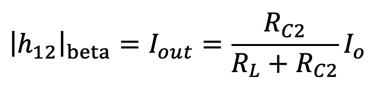
Most of the forward signal transmission comes from the feedforward gain stage and not through the feedback network. Using h-parameter terminology, this is expressed as:
(8.2)
![]()
Most of the signal that is fed back and mixed at the input to the amplifier comes from the feedback network and not through the feedforward gain stage. With h-parameter terminology this is expressed as:
(8.3)
![]()
With the aid of Spice let us compute the two-port hybrid-parameters of the feedforward and feedback networks shown in Fig. 8.4 and verify that the above assumptions are indeed satisfied. (We should expect that this is the case because the results generated by the feedback theory compare extremely well with those found directly from Spice.)
Using each circuit setup shown in Fig. 8.6, together with Spice, we can compute the h-parameters of both the feedforward gain stage and the feedback network shown in Fig. 8.4. As an example of one such case, the Spice deck for computing the h-parameters h11 and h21 for the feedforward gain stage is shown in Fig. 8.7. In this Spice deck the input port of the amplifier is driven by a one-amp AC signal I1 and the output port is short-circuited by a zero-valued voltage source V2. An AC analysis is asked to be performed at a single frequency of 1 Hz. (Any frequency will do, since the network contains no reactive elements). A .PRINT command is used to print out the voltage that appears at the input of the amplifier V(4) and the current that flows into the output port I(V2). Since the input current level is unity, both the voltage V(4) and the output current I(V2) will equal h-parameters h11 and h21, respectively. The results of this analysis are found in the output Spice file as follows:
|
**** AC ANALYSIS TEMPERATURE = 27.000 DEG C
FREQ VM(4) VP(4) IM(V2) IP(V2)
1.000E+00 1.110E+05 0.000E+00 1.000E+06 0.000E+00
|
Thus, h11=1.11 x 10⁵ V/A and h21= - 1 x 10⁶ A/A for the feedforward gain stage. (The sign of h21 is negative because the current monitored by V2 is positive and in opposite direction to the current denoted by I2 in Fig. 8.6. Recall that a current is considered positive when it flows from the positive to negative terminal of a voltage source.
|
Fig. 8.6: Hybrid-parameter representation of an arbitrary two-port network, and circuit setup for computing individual h-parameters.
|

The same approach is also used to compute the remaining two parameters, h12 and h22. One simply modifies the previous Spice deck by altering the two source statements given there. First, the level of current source I1 is set to zero and voltage source V2 is set to have a one-volt level according to the following:
|
I1 0 4 DC 0A AC 0A V2 1 0 DC 0V AC 1V.
|
The AC analysis request, together with the .PRINT command, remain the same. The results then computed by Spice are as follows:
|
**** AC ANALYSIS TEMPERATURE = 27.000 DEG C
FREQ VM(4) VP(4) IM(V2) IP(V2)
1.000E+00 1.000E-30 0.000E+00 1.501E-03 1.800E+02
|
In this case, the voltage V(4) corresponds to parameter h12 since the voltage driven into the second port is unity. As seen, it has a value of zero. This implies that no signal transmission occurs from the output of the feedforward gain stage back to its input. This is not too surprising given that there does not exist any direct connection between the input and output ports of the feedforward gain stage (see Fig. 8.4). Finally, parameter h22 is simply equal to the current supplied by V2 and is seen from above to be 1.501 x 10⁻³ A/V.
We can repeat this same type of analysis for the feedback network and arrive at the following set of h-parameters: h11=9.99 x 10+2 V/A, h12=9.99 x 10⁻² V/V, h21=-9.99 x 10⁻² A/A and h22=9.99 x 10⁻² A/V.
|
Table 8.4: The h-parameters of the feedforward and feedback networks shown in Fig. 8.4. |

The h-parameters for both the feedforward and feedback networks are compiled in Table 8.4 for easy comparison. Clearly, the above two assumptions, i.e., |h21|A >> |h21|beta and |h12|beta >> |h12|A are easily satisfied. Finally, it should be noted that resistances R11 and R22 that represent the loading of the feedback network on the feedforward network are given by R11=h21|beta and R22=1/h22|beta.
|
(a)
Fig. 8.4:(a) Feedforward gain stage of the noninverting amplifier circuit displayed in Fig. 8.3. (duplicate) |
Evaluating The h-Parameters Of Feedforward Gain Stage
** Circuit Description **
* input port conditions I1 0 4 DC 0A AC 1A V2 1 0 DC 0V AC 0V
* feedforward gain stage Rs 4 2 10k Ricm2 2 4 20Meg * amplifier Rid 2 3 100k Eamp 5 0 2 3 10k Ro 5 1 1k * load Rl 1 0 2k * feedback network input resistance R1i 3 0 1k R2i 3 0 1Meg Ricm2i 3 0 20Meg * feedback network output resistance R2o 1 30 1Meg R1o 30 0 1k Ricm2o 30 0 20Meg ** Analysis Requests ** .AC LIN 1 1Hz 1Hz ** Output Requests ** .PRINT AC Vm(4) Vp(4) Im(V2) Ip(V2) .end
Fig. 8.7: The Spice input file for calculating h-parameters h11 and h21 of the feedforward gain stage of the noninverting amplifier displayed in Fig. 8.4(a). The remaining two h-parameters h12 and h22 are found by setting the input level of I1 to zero and the output voltage source V2 to one-volt. Everything else remains the same.
|
|
(a)
|
(b)
|
|
|
Fig. 8.8: (a) A broadband amplifier composed of a feedback triple. The biasing circuitry is not shown (b) small-signal equivalent. |
||


8.2.2 Current-Sampling Series-Mixing Topology
The next example, shown in Fig. 8.8(a), illustrates a cascade of three transistors in a current-sampling series-mixing feedback configuration known as a feedback triple. This particular amplifier was presented as Example 8.2 in Sedra and Smith where the biasing circuit has been purposely left off the schematic. However, we are given enough biasing information from which to calculate the small-signal equivalent circuit of each transistor. We summarize the small-signal equivalent circuit parameters of each transistor below:
|
Q1 @ IC=0.6 mA: rp1=4.167 kOhm, gm1=24 mA/V Q2 @ IC=1.0 mA: rp2=2.5 kOhm, gm2=40 mA/V Q3 @ IC=4.0 mA: rp3=625 kOhm, gm3=160 mA/V
|
Using the above information, we can replace each transistor in Fig. 8.8(a) by its small-signal equivalent as shown in Fig. 8.8(b). Recognizing that the feedback network includes resistors RE1, RE2 and RF, we can apply the loading rules presented by Sedra and Smith and separate the feedforward circuit from the feedback circuit. These two circuits are given in Fig. 8.9. It is important to note that the current denoted as the output is not the actual current that is sampled and fed back to mix with the input signal, but rather a very close approximation to it. As we shall see, this approximation is reasonable for predicting the closed-loop signal gain Af of the amplifier, but incorrectly predicts the output resistance Rof.
|
(a)
(b)
Fig. 8.9: Isolated network portions of the broadband amplifier circuit: (a) feedforward network; (b) feedback network. |
Example 8.2: Feedforward Circuit Of Broadband Amplifier
** Subcircuits ** * small-signal equivalent transistor circuits .subckt Q1 1 2 3 rpi 2 3 4.1667k Gt 1 3 2 3 24m .ends .subckt Q2 1 2 3 rpi 2 3 2.5k Gt 1 3 2 3 40m .ends .subckt Q3 1 2 3 rpi 2 3 625 Gt 1 3 2 3 160m .ends
** Main Circuit ** * input signal Vi' 3 0 DC 0V * broadband amplifier * 1st stage Xt1 2 3 4 Q1 Rc1 2 0 9k * 2nd stage Xt2 5 2 0 Q2 Rc2 5 0 5k * 3rd stage Xt3 7 5 8 Q3 Rc3 6 7 600 * input resistance of feedback network Re1i 4 0 100 Rfi 4 41 640 Re2i 41 0 100 * output resistance of feedback network Re1o 81 0 100 Rfo 81 8 640 Re2o 8 0 100 * short-circuit output port Vout 0 6 0 ** Analysis Requests ** * calculate signal gain A=I(Vout)/Vi', Ri and Ro. .TF I(Vout) Vi' ** Output Requests ** * none required .end
Fig. 8.10: The Spice input file for calculating the signal gain A, and the input and output resistances (Ri and Ro), of the feedforward network of the broadband amplifier displayed in Fig. 8.9(a).
|


The Spice input file describing the feedforward circuit shown in Fig. 8.9 is listed below in Fig. 8.10. Notice here that we are using a zero-valued voltage source to form the short-circuit output. The current flowing through this voltage source can then be monitored. In a manner identical to that used in the voltage-sampling series-mixing case, we can obtain the signal gain Io' / Vi', Ri and Ro, directly using the built-in transfer function command (.TF) of Spice. These results, as calculated by Spice, are summarized in Table 8.5, together with the parameters for the feedback network obtained through hand analysis.
|
Table 8.5: Parameters of the feedforward and feedback circuit shown in Fig. 8.9 as calculated by Spice.
|
Table 8.6: Network parameters of the broadband amplifier circuit shown in Fig. 8.8 as calculated by Spice and through the application of feedback theory.
|


Using the results compiled in Table 8.5 and the theory developed for series-series feedback networks in Sedra and Smith (also seen summarized in Table 8.1), we can compute the signal gain Af and, the input and output resistances (Rif and Rof) of the small-signal equivalent circuit of the broadband amplifier displayed in Fig. 8.8. These results are listed in Table 8.6 and compared with the results calculated by direct analysis of the circuit shown in Fig. 8.8. The Spice input listing for the direct calculations is very similar to that given in Fig. 8.10 for the feedforward network and is therefore not shown here. The results predicted by feedback theory seem to agree quite closely with those computed directly with Spice.
If we repeat the above analysis with for the output resistance of each transistor included, specifically assuming that each has an Early voltage of 100 V (i.e., r0=167 kOhm, ro2=100 kOhm, and ro3=25 kOhm), then we find using Spice that the open-loop gain A=19.68 A/V, the feedback factor beta=11.9 V/A, and the input and output resistances are Ri=12.96 kOhm and Ro=65.91 kOhm, respectively. According to feedback theory, the closed-loop gain will then be Af=83.68 mA/V, the input resistance Rif=3.048 MOhm and the output resistance Rof=15.50 MOhm. When compared to the results computed directly by Spice, i.e., Af=82.77 mA/V, Rif= 2.603 MOhm and Rof=2.183 MOhm, we see that the signal gain Af is quite close to that computed by Spice. This is in contrast with the input resistance Rif and output resistance Rof predicted by feedback theory. In the case of the input resistance, the value predicted by feedback theory is about 17% larger than the value predicted by Spice. The reason for this discrepancy can be traced back to the fact that the input port of the feedforward network is not truly in series with the input port of the feedback network as was assumed in the development of the feedback theory for current-sampling series-mixing networks. Specifically, note that the current that flows into the input terminal of the feedforward network, Ii seen in Fig. 8.8, is not the same current that is eventually fed into the input port of the feedback network. The latter is instead (1+ gm1} rp1) Ii or (1 + beta) Ii. Although these two currents are dramatically different, in the ratio of 1:80 for the parameter values used above for gm1 and rp1, the error that this causes in the estimate of the input resistance of the closed-loop amplifier is relatively small at 17%.
In the case of the output resistance of the closed-loop amplifier, the value predicted by feedback theory is about 7 times larger than that computed by Spice; albeit, the actual output resistance has increased with the feedback applied, as expected. The reason for this large error is due to the fact that the current-sampling action is not taking place at the designated output port, that being in series with the collector of Q3, instead it is actually taking place on the emitter side of Q3.
If we re-perform the above feedback analysis on the original amplifier with the output port designated in series with the emitter of Q3 as shown in Fig. 8.11(a) then we should find that the output resistance computed directly by Spice will better agree with that estimated using feedback theory. Consider the small-signal equivalent circuit of the feedforward portion of the amplifier, shown in Fig. 8.11(b). Let us compute the signal gain, and the input and output resistance using Spice. The corresponding Spice deck is provided in Fig. 8.12. A transfer function (.TF) analysis is requested to be performed and the results of this analysis are provided below:
|
**** SMALL-SIGNAL CHARACTERISTICS
I(Vout)/Vi = 1.988E+01
INPUT RESISTANCE AT Vi = 1.296E+04
OUTPUT RESISTANCE AT I(Vout) = 1.426E+02
|
Here we see that A=19.88 A/V, Ri=12.9 kOhm and Ro=142.6 Ohm.
The feedback network portion of the original amplifier is identical to that seen previously. It is shown in Fig. 8.1(c) for completeness. The feedback factor beta was previously found to be 11.9 V/A. (Also, R11=88.1 Ohm and R22=88.1 Ohm.)
|
(a)
|
(b)
|
|
(c)
Fig. 8.11: (a) Designating the output port of the broadband amplifier in series with the emitter of Q3 to coincide with the port at which the current sampling is taking place. (b) Small-signal equivalent circuit of the feedforward portion of the amplifier. (c) Feedback network.
|
|


|
Table 8.7: Network parameters of the broadband amplifier circuit shown in Fig. 8.11(a) with the emitter current of Q3 as the output signal.
|
Table 8.8: The z-parameters of the feedforward and feedback networks shown in Fig. 8.11.
|


According to feedback theory the closed-loop signal gain Af is then 83.68 mA/V, the input resistance Rif equals 3.08 MOhm and the output resistance Rof is 33.88 kOhm. The first two parameters, Af and Rif are essentially the same as before when the output port was designated in series with the collector of Q3. The output resistance, however, is quite different from that seen previously but this should be expected given that the output port is now found on the emitter side of Q2. When the output resistance of the amplifier seen in Fig. 8.11(a) is computed directly with Spice, we obtain 33.90 kOhm. This result seems to now agree quite closely with the value predicted by feedback theory. Thus, re-assuring us that the feedback theory is consistent with what is observed in practice. The results of this analysis are summarized in Table 8.7.
|
(a)
Fig. 8.11: (a) Designating the output port of the broadband amplifier in series with the emitter of Q3 to coincide with the port at which the current sampling is taking place. (duplicate) |
Open-Loop Portion Of Broadband Amplifier (Revised Output Port)
** Subcircuits ** * small-signal equivalent transistor circuits .subckt Q1 1 2 3 rpi 2 3 4.1667k Gt 1 3 2 3 24m ro 1 3 167k .ends .subckt Q2 1 2 3 rpi 2 3 2.5k Gt 1 3 2 3 40m ro 1 3 100k .ends .subckt Q3 1 2 3 rpi 2 3 625 Gt 1 3 2 3 160m ro 1 3 25k .ends
** Main Circuit ** * input signal Vi' 3 0 DC 0V * broadband amplifier * 1st stage Xt1 2 3 4 Q1 Rc1 0 2 9k * 2nd stage Xt2 5 2 0 Q2 Rc2 0 5 5k * 3rd stage Xt3 7 5 80 Q3 Rc3 7 0 600 * input resistance of feedback network Re1i 4 0 100 Rfi 4 41 640 Re2i 41 0 100 * output resistance of feedback network Re1o 81 0 100 Rfo 81 8 640 Re2o 8 0 100 * monitor output current Vout 80 8 0 ** Analysis Requests ** .TF I(Vout) Vi' ** Output Requests ** * none required .end
Fig. 8.12: The Spice input file for calculating the signal gain A, and the input and output resistances (Ri and Ro), of the feedforward circuit with the emitter current of Q3 designated as the output signal as depicted in Fig. 8.11.
|

To further confirm the validity of the above results, the z-parameters of both the feedforward gain stage and feedback network are listed in Table 8.8. Here we see that the forward transmission through the feedback network is much smaller than that through the feedforward circuit, i.e., |z21|A >> |z21|beta. Conversely, the transmission from the output to the input of the feedforward gain stage is much less than the corresponding transmission through the feedback network, i.e., |z12|beta >> |z12|A. Finally, note that R11=z11|beta and R22=z22|beta.
|
(a)
Fig. 8.13: A single-stage amplifier circuit. An example of a voltage-sampling shunt-mixing feedback amplifier topology. |
(a)
(b)
Fig. 8.14: Isolated network portion of the amplifier circuit shown in Fig. 8.13: (a) feedforward gain stage without the biasing network shown; (b) feedback network.
|
|
Example 8.3: Voltage-Sampling Shunt-Mixing Voltage Amplifier Circuit (Closed-Loop)
** Circuit Description ** * power supply Vcc 1 0 DC +12V * input signal source (set to zero for operating point information) Is 0 3 DC 0A Rs 3 0 10k * amplifier circuit Rc 1 2 4.7k Q1 2 3 0 Q2N2222A * feedback circuit Rf 2 3 47k * transistor model statement for 2N2222A .model Q2N2222A NPN (Is=14.34f Xti=3 Eg=1.11 Vaf=74.03 Bf=255.9 Ne=1.307 + Ise=14.34f Ikf=.2847 Xtb=1.5 Br=6.092 Nc=2 Isc=0 Ikr=0 Rc=1 + Cjc=7.306p Mjc=.3416 Vjc=.75 Fc=.5 Cje=22.01p Mje=.377 Vje=.75 + Tr=46.91n Tf=411.1p Itf=.6 Vtf=1.7 Xtf=3 Rb=10) ** Analysis Requests ** .OP .TF V(2) Is ** Output Requests ** * none required .end
Fig. 8.15: The Spice input file for calculating the DC operating point information of transistor Q1 in the closed-loop amplifier shown in Fig. 8.13. Also included, for future reference, is a transfer function command (.TF) for calculating the gain A and the input and output resistances Rif and Rof.
|
|


8.2.3. Voltage-Sampling Shunt-Mixing Topology
In Fig. 8.13 we display a single-stage common-emitter amplifier with feedback resistor Rf. This particular circuit was presented by Sedra and Smith, 3rd Edition, in Example 8.3 of their text as an example of an amplifier having a voltage-sampling shunt-mixing topology. Here we shall decompose the feedback amplifier into its feedforward and feedback portions and analyze the individual circuits to estimate the behavior of the closed-loop amplifier. However, unlike the example in Sedra and Smith, we shall assume that Q1 is the commercial npn discrete transistor 2N2222A. This will complicate our analysis because the small-signal model of this transistor is much more complicated than that assumed by Sedra and Smith. Fortunately, using the following approach, the details of the small-signal equivalent circuit of the transistor will be kept hidden inside the computer -- thus avoiding tedious manipulations of the small-signal equivalent circuit and, more importantly, avoiding the necessity of making simplifying approximations and the corresponding loss of accuracy.
Consider applying the separation rules for shunt-shunt amplifier networks presented in Section 8.6 of Sedra and Smith to an assumed small-signal equivalent circuit of the amplifier shown in Fig. 8.13. To avoid complicating the schematics of the feedforward and feedback networks, we shall represent the small-signal equivalent circuit of the transistor by a single transistor symbol. In addition, the DC supplies will also be set to zero, as is always the case when working with small-signal circuit equivalents of transistor circuits. The result is the feedforward gain stage and the feedback network illustrated in Fig. 8.14.
To determine the small-signal model parameters of the transistor we shall first run a DC operating point (.OP) analysis on the original amplifier circuit shown in Fig. 8.13. The corresponding Spice input deck is shown in Fig. 8.15. Here we shall calculate both the DC operating point of Q1, and for future use, the gain A=Vo/Is, and the input and output resistances Rif and Rof. The bias conditions and transfer function characteristics as calculated by Spice are provided below:
|
**** SMALL SIGNAL BIAS SOLUTION TEMPERATURE = 27.000 DEG C *************************************************************************
NODE VOLTAGE NODE VOLTAGE NODE VOLTAGE NODE VOLTAGE
( 1) 12.0000 ( 2) 4.2056 ( 3) .6567
VOLTAGE SOURCE CURRENTS NAME CURRENT
Vcc -1.658E-03
TOTAL POWER DISSIPATION 1.99E-02 WATTS
**** OPERATING POINT INFORMATION TEMPERATURE = 27.000 DEG C *************************************************************************
**** BIPOLAR JUNCTION TRANSISTORS
NAME Q1 MODEL Q2N2222A IB 9.84E-06 IC 1.58E-03 VBE 6.57E-01 VBC -3.55E+00 VCE 4.21E+00 BETADC 1.61E+02 GM 6.09E-02 RPI 2.90E+03 RX 1.00E+01 RO 4.90E+04
**** SMALL-SIGNAL CHARACTERISTICS
V(2)/Is = -4.305E+04
INPUT RESISTANCE AT Is = 1.807E+02
OUTPUT RESISTANCE AT V(2) = 3.303E+02
|
Now that the small-signal model of transistor Q1 is known, we could use it in place of the transistor in the feedforward network of Fig. 8.14, in much the same way that was demonstrated in the previous example. Instead, a more elegant means of performing the required analysis is to externally bias the transistor using a current source to set the base current and a voltage source to set the collector-emitter voltage. Several AC analyses are then performed on the circuit to determine the signal gain, and the input and output resistances. To ensure that the transistor is properly biased and that the external bias sources do not interfere with the circuit small-signal operation, a large-valued decoupling capacitor C1 is added to the circuit to ensure that all the dc current supplied by the current source goes into the base of the transistor. Similarly, a large-valued inductor L2 is placed in series with the voltage source to block any AC current that would flow through the zero-source-resistance voltage source. This approach is depicted in Fig. 8.16. This method enables the details of the transistor small-signal model to be kept inside the computer where the greatest numerical precision is maintained.
|
Fig. 8.16: Feedforward circuit with transistor Q1 biased with an external current source IB and voltage source VCE. Infinite-valued decoupling capacitor C1 causes all the current supplied by IB to go into the base of Q1 but behaves as a short circuit for input AC signals. The infinite-valued inductor L2 acts as a short-circuit at DC allowing the voltage source VCE to set the voltage at the collector of Q1 but acts as an open circuit for any AC signal.
|
Example 8.3: Feedforward Portion Of Shunt-Shunt Amplifier
** Circuit Description ** * input signal source Ii' 0 3 AC 1A Rs 3 0 10k * amplifier circuit with isolated biasing network Rc 2 0 4.7k Q1 2 30 0 Q2N2222A C1 3 30 1GF L2 1 2 1GH IB 0 30 DC 9.84uA VCE 1 0 DC +4.21V * input and output resistance of feedback circuit Rf1 3 0 47k Rf2 2 0 47k * transistor model statement for 2N2222A .model Q2N2222A NPN (Is=14.34f Xti=3 Eg=1.11 Vaf=74.03 Bf=255.9 Ne=1.307 + Ise=14.34f Ikf=.2847 Xtb=1.5 Br=6.092 Nc=2 Isc=0 Ikr=0 Rc=1 + Cjc=7.306p Mjc=.3416 Vjc=.75 Fc=.5 Cje=22.01p Mje=.377 Vje=.75 + Tr=46.91n Tf=411.1p Itf=.6 Vtf=1.7 Xtf=3 Rb=10) ** Analysis Requests ** .OP .AC LIN 1 1Hz 1Hz ** Output Requests ** .Print AC Vm(2) Vp(2) Vm(3) Vp(3) .end
Fig. 8.17: The Spice input file for calculating the signal gain A=Vo'/Ii' and input resistance Ri=V(3)/Ii' of the feedforward circuit displayed in Fig. 8.16.
|

To convince the reader that this method does indeed maintain the correct transistor bias point, and therefore result in the same small-signal model as before, the small-signal model of the transistor in the circuit arrangement depicted in Fig. 8.16 was computed using Spice. The results found are as follows:
|
**** BIPOLAR JUNCTION TRANSISTORS
NAME Q1 MODEL Q2N2222A IB 9.84E-06 IC 1.58E-03 VBE 6.57E-01 VBC -3.55E+00 VCE 4.21E+00 BETADC 1.61E+02 GM 6.09E-02 RPI 2.90E+03 RX 1.00E+01 RO 4.90E+04
|
Comparing these results with those computed from the original amplifier, we see that they are in perfect agreement to the 3 digits provided.
We are now ready to use Spice to calculate the gain and resistance parameters of the feedforward network of the amplifier. We apply a one-amp AC current signal of 1 Hz frequency and with the aid of Spice compute the output voltage V(2) and input voltage V(3) (see labeled nodes in Fig. 8.16). Because the input current level is unity, the signal gain is simply given by V(2), and likewise, the input resistance is given directly by V(3). The Spice input deck for this situation is listed in Fig. 8.17.
The results of this simulation are:
|
FREQ VM(2) VP(2) VM(3) VP(3)
1.000E+00 5.125E+05 1.800E+02 2.150E+03 -7.889E-04
|
Thus, the signal gain is A=-512.5 kV/A and the input resistance Ri is 2.15 kOhm.
In a similar manner, the output resistance is computed by applying a one-amp AC current signal to the output port of the feedforward circuit with Ii'=0 A and calculating Ro=V(2). The Spice results of this calculations are:
|
FREQ VM(2) VP(2)
1.000E+00 3.930E+03 -7.114E-04
|
Thus, the output resistance Ro is 3.93 kOhm. The parameters of the feedback network should be obvious from Fig. 8.14. For easy viewing, we summarize the parameters of both the feedforward and feedback circuits in Table 8.9.
|
Table 8.9: Parameters of the feedforward and feedback circuits shown in Fig. 8.14 as calculated by Spice.
|
Table 8.10: Parameters of the feedback amplifier circuit shown in Fig. 8.13 as calculated by Spice and through the application of feedback theory.
|


|
Table 8.11: The y-parameters of the feedforward and feedback networks shown in Fig. 8.14.
|

Using the feedback theory developed by Sedra and Smith, 3rd Edition, for shunt-shunt feedback networks, we can calculate Af, Rif and Rof for the closed-loop amplifier shown in Fig. 8.13 using the formulae listed in Table 8.1. The results of these calculations are listed in Table 8.10. These results are also compared with those computed directly using Spice for the closed-loop amplifier. As evident, the results compare remarkably well.
To further confirm the validity of the above results, in Table 8.11 are listed the y-parameters of both the feedforward circuit and the feedback network. Here we see that the forward transmission through the feedback network is much smaller than that obtained by the feedforward network, i.e., |y21|A >> |y21|beta. Conversely, the transmission from the output to the input of the feedforward network is much less than the corresponding transmission through the feedback network, i.e., |y12|beta >> |y12|A. Finally, note that R11=1/y11|beta and R22=1/y22|beta.
8.2.4 Current-Sampling Shunt-Mixing Topology
As the final example of the four feedback amplifier topologies, we display in Fig. 8.18(a) a feedback amplifier circuit that is of the current-sampling shunt-mixing type. We shall carry out our analysis of this example in much the same way as that performed with the previous example. However, we shall assume that Q1 and Q2 are commercial npn transistors of the 2N3904 type. A similar example was presented in Sedra and Smith as Example 8.4 of their text; however, a slight change of the biasing circuitry was necessary to accommodate the 2N3904 type transistors. Although, the current Iout is ultimately the current of primary interest since it is this current that we are trying to stabilize with the application of negative feedback, we shall focus our attention on the collector current of Q2, denoted by Io. This is because Io closely approximates the emitter current of Q2 which is sampled by the feedback network on which the feedback theory of Sedra and Smith is based. Once Io is obtained, Iout is simply obtained from the following expression:
(8.4)
The circuit shown in Fig. 8.18(b) is the same circuit as in part (a) but the output port is re-arranged so that the collector current of Q2 becomes the output current.
|
(a)
|
(b)
|
|
Fig. 8.18: (a) Feedback amplifier incorporating a form of current-sampling shunt-mixing feedback. (b) Rearranging the output section of the amplifier so that the collector current of Q2 becomes the output current.
|
|


|
(a)
(b) Fig. 8.19: Isolated network portions of the amplifier circuit shown in Fig. 8.18: (a) feedforward network with external biasing shown; (b) feedback network.
|
Example 8.4: Feedforward Network Of Current-Sampling Shunt-Mixing Amplifier
** Circuit Description ** * input signal source Ii' 0 10 DC 0A AC 1A Rs 10 0 10k * output current (collector current of Q2) Vout 5 50 DC 0V AC 0V * power supply Vcc 1 0 DC +12V * amplifier circuit * 1st stage Q1 2 3 4 Q2N3904 Rc1 1 2 10k Re1 4 0 870 Ce 4 0 1GF Rb1 1 3 100k Rb2 3 0 15k * 2nd stage Q2 50 2 6 Q2N3904 Rc2 1 5 8k * decoupling capacitors Cc1 10 3 1GF Cc2 5 8 1GF * load Rl 8 0 1k * open feedback circuit * input side Rfi 3 72 10k Cfi 73 72 1GF Re2i 73 0 3.4k * output side Rfo 71 0 10k Cfo 6 71 1GF Re2o 6 0 3.4k * transistor model statement for 2N3904 .model Q2N3904 NPN (Is=6.734f Xti=3 Eg=1.11 Vaf=74.03 Bf=416.4 Ne=1.259 + Ise=6.734f Ikf=66.78m Xtb=1.5 Br=.7371 Nc=2 Isc=0 Ikr=0 Rc=1 + Cjc=3.638p Mjc=.3085 Vjc=.75 Fc=.5 Cje=4.493p Mje=.2593 Vje=.75 + Tr=239.5n Tf=301.2p Itf=.4 Vtf=4 Xtf=2 Rb=10) ** Analysis Requests ** .OP .AC LIN 1 1Hz 1Hz ** Output Requests ** .PRINT AC Im(Vout) Ip(Vout) Vm(10) Vp(10) .end
Fig. 8.20: The Spice input file for calculating the input -- output current gain and input resistance for the feedforward network shown in Fig. 8.19(a). |


The feedforward circuit, including the loading effects of the feedback network, is shown in Fig. 8.19(a). Here we should notice that because the feedback network is AC coupled, rearranging it does not affect the biasing conditions of either Q1 or Q2. Furthermore, because the input signal passes through a decoupling capacitor, we cannot obtain the three network parameters usually of interest here using the DC transfer function (.TF) analysis command of Spice. Instead we must use the approach presented in the previous example. That is, to obtain the signal gain Io'/Ii' and the input resistance Ri, we apply a one-amp AC signal to the input of the feedforward amplifier and calculate the output current Io', and voltage appearing across the input port (V(10)). The Spice input file for this particular circuit situation is shown listed in Fig. 8.20. The results of this AC analysis are then found in the output file as follows:
|
FREQ IM(Vout) IP(Vout) VM(10) VP(10)
1.000E+00 2.449E+02 1.800E+02 2.077E+03 -6.311E-04
|
Here we see that A=-244.9 A/A and Ri=2.077 kOhm.
In the case of the output resistance, this is obtained by applying a 1 V AC voltage source in series with the short-circuited output and setting the input current level to zero. The output resistance Ro is then simply the reciprocal of the current supplied by this voltage source. The previous Spice deck can be used to perform this by simply modifying the source statements for Ii' and Vout according to:
|
Ii' 0 10 DC 0A AC 0A Vout 5 50 DC 0V AC 1V. |
The analysis request and print statement remain unchanged.
On completion of Spice, one finds the following results in the output file:
|
FREQ IM(Vout) IP(Vout) VM(10) VP(10)
1.000E+00 3.413E-07 -1.800E+02 1.464E-11 -9.469E+01
|
The output resistance of the feedforward network is thus found to be Ro=2.930 MOhm.
The parameters associated with the feedback network shown in Fig. 8.18 are obvious and are summarized in Table 8.12. Also listed are the parameters associated with the feedforward circuit (calculated above).
|
Table 8.12: Parameters of the feedforward and feedback network shown in Fig. 8.19 as calculated by Spice.
|
Table 8.13: Parameters of the feedback amplifier circuit shown in Fig. 8.18 as calculated by Spice and through the application of feedback theory.
|


Finally, in Table 8.13, we compare several parameters of the closed-loop amplifier as calculated directly by Spice with those computed using feedback theory. As is evident, the signal gain and the input resistance are very close. However, the output resistance Rof calculated by Spice is about an order of magnitude less than that predicted by feedback theory. The reason for this can be traced back to a very early assumption where the current of interest, the collector current of Q2, was designated as the output current, where in fact, the emitter current of Q2 is actually the current that is being sampled and fed back to mix with the input signal. Now, it is generally true that the collector and emitter currents of a transistor are very close owing to the transistor a being nearly unity, and what can be said about one should apply to the other, such as the current gain Af. It is not true, however, that the theory of feedback networks derived in Sedra and Smith for computing the output resistance Rof applies to a port where the output signal is not the actual signal that is being sampled. This is certainly borne out by the results that we see in Table 8.13.
|
Fig. 8.21: Feedforward gain stage of the feedback amplifier of Fig. 8.18 with the output port re-designated to be in series with the emitter of transistor Q2 instead of in series with the collector of Q2 as was the case previously.
|

If we re-designate the output port as that which contains the emitter current of Q2 then we should find that Rif, Rof and Af will closely match those predicted by Spice. Consider the revised feedforward gain stage shown in Fig. 8.21. The input resistance, Ri is the same as that seen previously at 2.077 kOhm, the current gain Ai is almost the same as before at -246.6 A/A and the output resistance Ro is 2.639 kOhm. These results were all computed by Spice with an input file that is quite similar to that shown previously in Fig. 8.20 and is therefore not shown here.
Combining the open-loop parameters of the feedforward gain stage with the previously computed feedback network parameters, we obtain Af=-3.879 A/A, Rif=32.68 Ohm and Rof=167.7 kOhm. Comparing these with the results computed directly by Spice, i.e., Af=-3.879 A/A, Rif=32.65 Ohm and Rof=167.9 kOhm, we see that all three values agree quite closely with those predicted by feedback theory. Furthermore, we see that the current gain from the input to the emitter current of Q2 (-3.879 A/A) is exactly the same as the current gain from the input to the collector current of Q2 (-3.879 A/A), as expected since transistor a is nearly unity.
|
Table 8.14: The g-parameters of the feedforward and feedback networks shown in Fig. 8.21 and Fig. 8.19(b), respectively. |

To check the validity of the above results, the g-parameters of both the feedforward and feedback networks shown in Fig. 8.21 and Fig. 8.19(b), respectively, are shown listed in Table 8.14. Here we see that the forward transmission through the feedback network is about 1000 times smaller than the forward gain of the feedforward gain stage, i.e., |g21|A >> |g21|beta. Likewise, the reverse transmission through the feedback network is over five orders of magnitude larger than the transmission from the output to the input of the feedforward network, i.e., |g12|beta >> |g12|A. Therefore, we are justified in separating the closed-loop amplifier shown in Fig. 8.18 into two separate feedforward and feedback networks. Finally, note that R11=1/g11|beta and R22=g22|beta.
|
Fig. 8.22: Breaking the feedback loop of an amplifier at a point in the network which affects its DC bias.
|

8.3 Determining Loop Gain with Spice
An important parameter of feedback amplifiers is the loop gain A x beta. In this section we shall demonstrate a more direct approach to determining the loop gain using Spice than the network separation method employed in the previous section.
Consider determining the loop gain of the feedback amplifier circuit shown in Fig. 8.22. This is the same circuit presented in our previous example and the results found there can then be compared with the results obtained here. To determine the loop gain, the feedback loop of this amplifier must be broken in order to inject a signal into the loop. However, the circuit conditions of the loop must remain the same as when the loop was closed. This includes maintaining the same bias conditions on each transistor and terminating the feedback loop with the impedance seen by the loop under closed-loop conditions.
With regards to the circuit shown in Fig. 8.22, a convenient location for breaking the feedback loop is in the AC coupled feedback network. By doing so, the DC bias conditions of each transistor are not disturbed. However, in many circuit situations, the feedback network is directly coupled, and one therefore requires a method that is amenable to such situations.
Consider breaking the feedback loop at a location which disturbs the DC biasing of the circuit. Such a location is highlighted by a big {\bf X} in the circuit diagram of Fig. 8.22. By inserting a very large inductor in series with the terminals of the break, then the DC bias conditions of each transistor would remain invariant because the inductor behaves as a short circuit at DC. However, for AC signals, the large inductor presents a large impedance in series with the loop. For all intents and purposes, selecting a large inductor of say (for Spice purposes) 1 giga-henries opens the loop for almost all AC signals.
|
(a)
(b) Fig. 8.23: (a) Opening a feedback loop with a very large inductor Lt. The impedance seen by the feedback loop, and in which we must terminate the loop is found by calculating the current supplied by the AC coupled test voltage source Vt. (b) Feedback loop terminated in AC coupled load resistance Rt.
|
Computing The Loop Terminating Resistance Rt
** Circuit Description ** * input source set to zero for output impedance calculation Vs 11 0 DC 0 AC 0 Rs 11 10 10k * short-circuit output port Vout 0 9 0 * power supply Vcc 1 0 DC +12V * amplifier circuit * 1st stage Rc1 1 2 10k Q1 2 3 4 Q2N3904 Re1 4 0 870 Ce1 4 0 1GF Rb1 1 3 100k Rb2 3 0 15k * 2nd stage Rc2 1 5 8k Q2 5 21 6 Q2N3904 * decoupling capacitors Cc1 10 3 1GF Cc2 5 8 1GF * load Rl 8 9 1k * feedback circuit Re2 6 0 3.4k Rf 3 7 10k Cf 6 7 1GF * inject signal into feedback loop without disturbing DC bias Lt 2 21 1GH Cti 21 22 1GF Vt 22 0 AC 1V * transistor model statement for 2N3904 .model Q2N3904 NPN (Is=6.734f Xti=3 Eg=1.11 Vaf=74.03 Bf=416.4 Ne=1.259 + Ise=6.734f Ikf=66.78m Xtb=1.5 Br=.7371 Nc=2 Isc=0 Ikr=0 Rc=1 + Cjc=3.638p Mjc=.3085 Vjc=.75 Fc=.5 Cje=4.493p Mje=.2593 Vje=.75 + Tr=239.5n Tf=301.2p Itf=.4 Vtf=4 Xtf=2 Rb=10) ** Analysis Requests ** .AC LIN 1 1Hz 1Hz ** Output Requests ** * print resistance seen by Vt: Rt=V(22)/I(Vt) .PRINT AC Vm(22) Vp(22) Im(Vt) Ip(Vt) .end
Fig. 8.24: The Spice input file for calculating the input impedance Rt=V(22)/I(Vt) of the feedback loop for the amplifier circuit shown in Fig. 8.23(a).
|


To determine the impedance required to terminate the loop, we simply calculate the impedance seen looking into the terminal where the loop was broken. For this particular example, we apply a one-volt AC voltage signal Vt to the base of Q2 through a DC blocking capacitor as shown in Fig. 8.23(a), and calculate the current supplied by this source. The ratio Vt/It then gives the input impedance. Of course, these results will be frequency dependent, so we limit our discussion to midband frequencies where the input impedance is purely resistive. In this particular example, a frequency of 1 Hz is considered to be midband. The DC blocking capacitor is necessary to prevent the input voltage source from disturbing the DC bias conditions on Q2. Its value should be made large to minimize the voltage drop across it (for most purposes, a value of 1 giga-farads should suffice).
The Spice input file for determining the input impedance of the feedback loop is listed in Fig. 8.24. On completion of Spice, the following results are found in the Spice output file,
|
FREQ VM(22) VP(22) IM(Vt) IP(Vt)
1.000E+00 1.000E+00 0.000E+00 2.482E-06 1.800E+02
|
from which we can determine the input resistance to be 402.9 kOhm.
The output of the feedback loop can now be terminated in a resistance of 402.9 kOhm. A DC blocking capacitor is necessary, once again, to prevent this resistance from disturbing the amplifier’s DC biasing. This is illustrated in the circuit diagram shown in Fig. 8.23(b). Modifying the Spice input file given in Fig. 8.24 by attaching this resistance and capacitor combination to the output of the feedback loop allows us to calculate the loop gain. One simply adds the following two element statements:
|
Cto 2 23 1GF Rt 23 0 402.9k
|
and revises the output print statement as follows
.PRINT AC Vm(22) Vp(22) Vm(23) Vp(23).
The results of this Spice calculation are then found in the output file as follows:
|
FREQ VM(22) VP(22) VM(23) VP(23)
1.000E+00 1.000E+00 0.000E+00 5.954E+01 1.800E+02
|
Hence, one finds the loop gain Abeta=-Vr/Vt=59.54. Comparing this result with that obtained using the separation method performed in the last section, one finds A x beta=(-244.9)*(-0.2537)=62.13. Thus, both approaches result in reasonably close values for the loop gain.
|
(a)
|
(b)
|


Fig. 8.25: (a) Determining the open-circuit voltage transfer function TOC=VOC/Vt. (b) Determining the short-circuit current transfer function TSC=ISC/It.
An Alternative Method:
An alternative method for determining loop gain, and one that better lends itself to Spice, is due to Rosenstark [Rosenstark, 1986]. Without proof, the method of Rosenstark simply determines the loop gain by two independent calculations. The first involves calculating the voltage transfer function from the input of the broken loop to its output with the loop unterminated (i.e., Rt=¥). This we denote as the open-circuit transfer function, TOC. The other calculation involves finding the current transfer function from the input of the loop to its short-circuited output. This we call the short-circuit transfer function, TSC. We depict these two situations for an arbitrary broken feedback loop in Fig. 8.25. These two results are then combined to compute the loop transmission according to
(8.5)
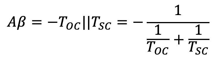
It is obvious from this formula that the smaller of the two transfer functions will dominate the loop gain.
The advantage of this approach over the previous method of terminating the feedback loop is that both TOC and TSC can be calculated over a wide range of frequencies without worrying about whether the loop is properly terminated with the correct impedance.
To demonstrate this approach, we shall return to the opened feedback loop of the last example shown in Fig. 8.23(a). Here the loop is shown unterminated and driven by a voltage source Vt. The Spice file for this particular situation was shown in Fig. 8.24 and can be used to calculate the open-circuit voltage VOC. Adding the following print statement to this file,
.PRINT AC Vm(22) Vp(22) Vm(2) Vp(2),
and re-submitting this file to Spice will result in the following open-circuit voltage in the Spice output file:
|
FREQ VM(22) VP(22) VM(2) VP(2)
1.000E+00 1.000E+00 0.000E+00 6.086E+01 1.800E+02 |
Thus, we obtain TOC=-60.86.
|
Fig. 8.26: Determining the short-circuit current transfer function TSC=ISC/It.
|
Computing The Short-Circuit Current Transfer Function
** Circuit Description ** * power supply Vcc 1 0 DC +12V * input source set to zero for output impedance calculation Vs 11 0 DC 0 AC 0 Rs 11 10 10k * amplifier circuit * 1st stage Rc1 1 2 10k Q1 2 3 4 Q2N3904 Re1 4 0 870 Ce1 4 0 1GF Rb1 1 3 100k Rb2 3 0 15k * 2nd stage Rc2 1 5 8k Q2 5 21 6 Q2N3904 * decoupling capacitors Cc1 10 3 1GF Cc2 5 8 1GF * load Rl 8 9 1k * output current Vout 0 9 DC 0 * feedback circuit Re2 6 0 3.4k Rf 3 7 10k Cf 6 7 1GF * inject signal into feedback loop Lt 2 21 1GH It 0 21 AC 1A Cto 2 23 1GF Vsc 23 0 0 * transistor model statement for 2N3904 .model Q2N3904 NPN (Is=6.734f Xti=3 Eg=1.11 Vaf=74.03 Bf=416.4 Ne=1.259 + Ise=6.734f Ikf=66.78m Xtb=1.5 Br=.7371 Nc=2 Isc=0 Ikr=0 Rc=1 + Cjc=3.638p Mjc=.3085 Vjc=.75 Fc=.5 Cje=4.493p Mje=.2593 Vje=.75 + Tr=239.5n Tf=301.2p Itf=.4 Vtf=4 Xtf=2 Rb=10) ** Analysis Requests ** .AC LIN 1 1Hz 1Hz ** Output Requests ** * print short-circuit current gain .PRINT AC Im(Vsc) Ip(Vsc) .end
Fig. 8.27: The Spice input file for calculating the short-circuit transfer function TSC=ISC/It in the opened feedback loop shown in Fig. 8.26.
|

To determine the short-circuit transfer function, we must remove the input voltage source Vt and replace it with an AC current source. In addition, we must also AC short-circuit the output port by adding a zero-valued voltage source in series with a large capacitor. The zero-valued voltage source provides the means of monitoring the short-circuit current. We depict this circuit arrangement in Fig. 8.26 and the corresponding Spice input file in Fig. 8.27. Submitting this file to Spice, results in the following short-circuit output current:
|
FREQ IM(Vsc) IP(Vsc)
1.000E+00 2.753E+03 1.800E+02 |
Therefore, we get TSC=-2753. Now from Eqn. (8.5), we calculate the loop gain to be 59.54 which is exactly the same as the loop gain calculated by the method which terminates the loop.
8.4 Stability Analysis Using Spice
From the loop gain, or more appropriately the loop transmission, one can determine the stability of a feedback amplifier. Consider the filter circuit shown in Fig. 8.28(a) where the feedback loop is frequency dependent and the amplifier has unity gain (K=1). One possible point for breaking the loop is at the amplifier's input. This is probably the most convenient point in the loop because the loop is not loaded by the amplifier input and therefore the loop does not need to be terminated when it is opened. The loop transmission is then found by calculating the return voltage Vr, as indicated in Fig. 8.28(b), with a one-volt AC signal applied to the amplifier input. The sign of the input signal is made negative so that the loop transmission Abeta directly equals Vr (instead of -Vr). A Spice description of the circuit shown in Fig. 8.28(b) is given in Fig. 8.29. Here we are requesting an AC analysis of the circuit beginning at 1 Hz and extending up to 1 MHz. This range of frequency should be large enough to capture the important behavior of the loop transmission.
|
(a)
(b)
Fig. 8.28: (a) A 2nd-order filter circuit with a frequency-dependent feedback loop. (b) Opened feedback loop for calculating loop transmission.
|
Example 8.5: Calculating Loop Transmission Of 2nd Order Active Filter (K=1)
** Circuit Description ** * input signal source Vt 1 0 AC 1V 180degrees * filter circuit Egain 2 0 1 0 1 Inull 1 0 0 ; redundant connection * feedback network C1 2 3 1uF R1 3 0 159.15 R2 3 4 159.15 C2 4 0 1uF ** Analysis Requests .AC DEC 10 1Hz 1MegHz ** Output Requests ** .PLOT AC VdB(4) Vp(4) .PROBE .end
Fig. 8.29: The Spice input file for calculating the frequency-dependent loop transmission of the filter circuit shown in Fig. 8.28(b).
|


|
(a)
|
(b)
|


Fig. 8.30: Various forms of representing the loop transmission: (a) Bode plot (b) Nyquist plot.
|
(a)
|
(b)
|


Fig. 8.31: A Bode and Nyquist plot of the loop transmission of an unstable filter (K=5). Here the Nyquist plot encircles the critical point of (--1,0).
On completion of Spice, a plot of both the magnitude and phase of the loop transmission will be found in the output file. These results, as drawn by the Probe facility of PSpice, are on display in Fig. 8.30(a). Reviewing these results, we see that the gain margin is ~10 dB, suggesting that the filter circuit will be stable when the loop is closed. Equivalently, we can use these results to draw a Nyquist plot and show that the critical point (--1,0) is not encircled. This we have done in Fig. 8.30(b), thus confirming our intuition.
As an example of an unstable filter circuit, consider increasing the gain of the amplifier in the filter circuit of Fig. 8.28(a) to 5 (i.e., K=5). Modifying the Spice input file listed in Fig. 8.29 to reflect this change and re-running this file, will result in the new Bode plot shown in Fig. 8.31(a). Here we observe that at the 180°-phase frequency, the loop gain will be greater than unity, indicating unstable performance. Alternatively, a Nyquist plot can also be drawn using this same frequency information. The result is shown in Fig. 8.31(b). Here we see that the critical point (-1,0) is encircled. Also confirming that the filter circuit will be unstable when the loop is closed.
|
(a)
Fig. 8.28: (a) A 2nd-order filter circuit with a frequency-dependent feedback loop. (duplicate)
|
Closed-Loop Transient Response Of Stable Filter Circuit (K=1)
** Circuit Description **
* input signal source Vi 4 0 sin( 0V 1V 1kHz )
* filter circuit Egain 2 0 1 0 1 * feedback stage C1 2 3 1uF R1 3 4 159.15 R2 3 1 159.15 C2 1 0 1uF
** Analysis Requests .TRAN 10us 5ms 0ms 10us ** Output Requests ** .PLOT TRAN V(2) V(4) .probe .end
Fig. 8.32: The Spice input file for calculating the transient response of the filter circuit shown in Fig. 8.28(a) to a one-volt 1 kHz sinewave input.
|
|
Fig. 8.33: The transient response to a one-volt 1 kHz sinewave signal applied to the input of the filter circuit shown in Fig. 8.28(a) with K=1 and K=5. The top curve represents the input sinewave signal; the middle curve represents the output signal from the stable filter circuit (K=1); the bottom curve represents the output signal from the unstable filter circuit (K=5).
|
Fig. 8.34: Comparing the magnitude and phase response of a stable and an unstable filter circuit. The top graph displays the magnitude responses and the bottom graph displays the corresponding phase responses.
|


Before moving on, it would be highly instructive to investigate the closed-loop transient behavior of the two filter circuits discussed above, i.e., one stable and the other unstable. For the original filter circuit seen in Fig. 8.28(a) with K=1, a Spice input file is provided in Fig. 8.32. A one-volt peak amplitude sinewave signal of 1 kHz frequency is applied to the input terminal of the filter using the following Spice transient voltage source statement:
Vi 4 0 sin( 0V 1V 1kHz ).
A transient analysis is requested to be performed over 5 periods of the input signal (i.e., 5 ms) with 100 points collected per period of the input signal. The Spice command appears in the input file as follows:
.TRAN 10us 5ms 0ms 10us.
Finally, a .PLOT statement is used to observe both the input and output voltage signal:
.PLOT TRAN V(2) V(4).
Another Spice input file is created for the unstable filter circuit, i.e., K=5. This Spice file is almost identical to that seen in Fig. 8.32 with the simple modification of changing the amplifier gain to 5. This Spice file is concatenated on the end of the Spice file seen in Fig. 8.32 and then submitted as one file to Spice for processing. On completion of Spice, the transient response of each filter circuit is shown in Fig. 8.33. The top curve illustrates the sinewave signal applied to the input of each filter circuit. The middle waveform represents the signal that appears at the output of the stable filter circuit. As is evident, except for an amplitude and phase shift, this signal is identical to the input signal shown above it. In contrast, the signal appearing at the output of the unstable filter in the bottom-most graph bears no resemblance to the input sinewave signal at all. Moreover, the level of this output signal has approached 1010 V in about 3 ms. Clearly, this is unstable behavior. If Spice were left running much longer than 3 ms, numbers stored within the computer would get so large that they would overflow the internal registers of the computer. This then causes Spice to terminate the present Spice job.
As a final point, novice users of Spice sometimes think that if Spice can produce a frequency response plot of a closed-loop circuit, then that circuit must be stable. This is certainly not true. To demonstrate this, in Fig. 8.34 the magnitude and phase response of both the stable and the unstable closed-loop filter circuits are shown. These results were computed using a revised version of the Spice deck shown in Fig. 8.32. The input signal source was replaced by an AC signal source having the following form:
Vi 4 0 AC 1V,
and the transient analysis command seen there was replaced with the following AC analysis command:
.AC DEC 10 1Hz 1MegHz.
The following .PLOT command was also added:
.PLOT AC VdB(2).
Returning to Fig. 8.34, we see that both circuits, regardless of stability, have a corresponding magnitude and phase response. The magnitude response behavior of each filter is quite similar, except for a vertical shift as a result of the different amplifier gains. The greatest difference in the behavior of the two filters appears in their phase. The stable filter has a phase response that goes from 0 degrees to -180 degrees as the input signal frequency increases from DC. In contrast, the phase response of the unstable filter goes from 0 degrees to +180 degrees with increasing input signal frequency. The reason for this behavior should be obvious; in the first case, the poles appear on the left-hand side of the jw axis in the s-plane, and in the latter, they appear on the righthand side. From the location of the poles, the stability of the network can be easily deduced. Unfortunately, in more complicated circuits having many more poles and zeros, the phase behavior of the amplifier would not so clearly identify poles in the righthand side of the s-plane. In general, without any special insight into circuit behavior, the stability of a circuit cannot be determined from the frequency response of the closed-loop circuit. It is therefore recommended that the stability of a closed-loop circuit be investigated using a Spice transient analysis (preferably, using a step input signal that is rich in a wide-band of signal frequencies, as opposed to a single sinewave input signal as used in this example).
8.5 Investigating the Range of Amplifier Stability
In this section we shall investigate the range of stability of an amplifier with complex frequency response behavior using Bode plots generated by Spice. The same amplifier characteristics that were used in Section 8.10 of Sedra and Smith, 3rd Edition, will be used here. This will enable our readers to correlate the results given here with those calculated by hand. Furthermore, a Spice transient analysis will be used to verify circuit stability.
|
(a)
(b)
Fig. 8.35: (a) A differential-input amplifier having an open-loop response A(s) with three separate poles. (b) Small-signal equivalent circuit.
|
Open-Loop Amplifier Characteristics
** Circuit Description **
* input signals
Vin+ 1 0 AC 1V Vin- 2 0 AC 0V
* open-loop amplifier configuration * connections: 1 2 3 * | | | * in+ | | * in- | * out
* first stage Rid 1 2 1MegOhm Gm1 4 0 1 2 4.93m R1 4 0 15.915k C1 4 0 100pF * second stage Gm2 5 0 4 0 40m R2 5 0 31.83k C2 5 0 5pF * output buffer stage E3 6 0 5 0 1 Ro 6 3 100 Co 3 0 159.15pF
** Analysis Requests .AC DEC 10 1Hz 100MegHz ** Output Requests ** .PLOT AC VdB(3) Vp(3) .PROBE .end
Fig. 8.36: The Spice input file for calculating the open-loop frequency response behavior of the three-pole amplifier circuit shown in Fig. 8.35(b). |


As an example, consider the differential-input amplifier shown in Fig. 8.35(a) with an input-output transfer function A(s). Let us assume that A(s) is characterized by three real poles distributed along the negative axis of the s-plane at frequency locations of: 0.1 MHz, 1 MHz and 10 MHz. Further, let the DC gain of the amplifier be 105 V/V or 100 dB. The open-loop transfer function A(s) can then be described by the following:
(8.6)
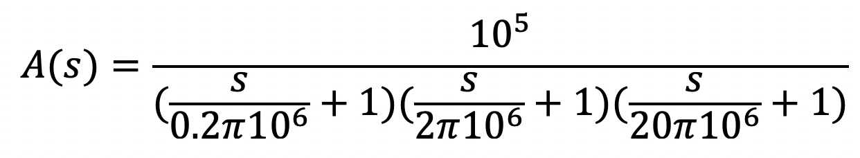
Figure 8.35(b) shows a small-signal equivalent circuit of a typical three stage amplifier configuration. It consists of two transconductance gain stages and an output buffer stage. With the following component values, the transfer function of this small-signal equivalent circuit is described by that given in Eqn. (8.6):
|
1st Stage: Rid=1 MOhm, gm1=4.93 mA/V, R1=15.915 kOhm, C1=100 pF
2nd Stage: gm2=40 mA/V, R2=31.83 kOhm, C2=5 pF
3rd Stage: Ro=100 Ohm, Co=159.15 pF |
To observe the frequency response behavior of this amplifier, we use the Spice input file shown listed in Fig. 8.36. The amplifier input is excited with a one-volt AC signal applied to the positive input terminal. The negative input terminal is simply set to 0 V. An AC analysis is then requested between 1 Hz and 100 MHz. Both the magnitude and phase of the signal appearing at the amplifier output are to be plotted. Since the input signal is set at one-volt, the magnitude and phase of this output signal also represent the magnitude and phase of the input-output transfer function A(s).
|
Fig. 8.37:
Magnitude and phase response of the differential-input amplifier shown in
Fig. 8.35 with
|

The results of the Spice analysis have been collected and plotted in Fig. 8.37. Here we see that the gain of the amplifier is 100 dB at low frequencies and has a 3-dB frequency located quite close to 100 kHz. Near the unity-gain frequency of 46 MHz, the slope of the magnitude response is seen to be about -60 dB-per-decade. The phase response of this amplifier is provided in the plot shown below the magnitude response. The majority of the phase shift occurs between 10 kHz and 100 MHz; one decade below the location of the first pole and one decade above the highest frequency pole. The frequency at which the phase shift equals 180° is 3.31 MHz; this was found using the cursor facility of Probe.
For a unity feedback factor independent of frequency, i.e., beta=1, the loop gain Abeta would have a gain margin of GM =-58.4 dB, or alternatively, a phase margin of PM = -76.5°. Clearly, connecting this amplifier in a unity-gain configuration would result in unstable operation. In fact, it is not until the loop gain drops below 41.6 dB (e.g., Ao - GM = 100 dB - 58.4 dB), would the closed-loop amplifier configuration result in stable operation. This simply corresponds to the point at which the gain margin reduces to zero for a feedback factor 20log(1/beta)= 58.4 dB, or beta = 1.202 x 10⁻³. Thus, stable circuit operation using the amplifier described above is maintained in a closed-loop configuration for frequency independent feedback factors beta being less than 1.202 x 10⁻³. Correspondingly, since the closed-loop gain under large loop gain conditions, is approximately 1/beta, the amplifier described above is limited to applications requiring a closed-loop gain greater than 831.82 V/V or 58.4 dB.
|
Fig. 8.38: A noninverting amplifier configuration with closed-loop gain Af = (1 + RB/RA). The differential-input amplifier has transfer function A(s) defined by Eqn. (8.6) and beta = RA/(RA + RB).
|
Step Response Of A Noninverting Amplifier With A Gain Of +2 V/V
** Subcircuits **
.subckt diffopamp 1 2 3 * open-loop amplifier configuration * connections: 1 2 3 * | | | * in+ | | * in- | * out * first stage Rid 1 2 1MegOhm Gm1 4 0 1 2 4.93m R1 4 0 15.915k C1 4 0 100pF * second stage Gm2 5 0 4 0 40m R2 5 0 31.83k C2 5 0 5pF * output buffer stage E3 6 0 5 0 1 Ro 6 3 100 Co 3 0 159.15pF .ends diffopamp
** Main Circuit **
* one-volt step input signal Vstep 1 0 PWL (0 0V 1ns 0V 2ns 1mV 1s 1mV) * noninverting amplifier Xdiffamp 1 2 3 diffopamp RA 2 0 100k RB 2 3 100k
** Analysis Requests .TRAN 100ns 12us 0s 100ns ** Output Requests ** .PLOT TRAN V(3) V(1) .PROBE .end
Fig. 8.39: The Spice input file for calculating the step response of a noninverting amplifier having a closed-loop gain of +2 V/V. The differential-input amplifier is modeled by the small-signal equivalent circuit shown in 8.35(b).
|

To verify the above result, let us investigate the step response of the noninverting amplifier configuration shown in Fig. 8.38 having a closed-loop gain of +2 V/V and +1001 V/V. The differential amplifier will be assumed to be modeled after the small-signal equivalent circuit shown in Fig. 8.35(b). In the first case, we shall select RA to be 100 kOhm, and in the second case, RA will be assigned a value of 100 Ohm. For both cases, RB will be set equal to 100 kOhm. The Spice deck for the amplifier having a gain of +2 V/V is shown listed in Fig. 8.39. The Spice deck for the other amplifier is identical except for the change in the resistor value of RA. A 1 mV step input is applied to the input of the closed-loop amplifier. Hence, we should expect a 2-mV output signal if the amplifier is stable.
The step input signal is approximated by a series of piece-wise linear segments described to Spice using the PWL source statement. It appears in the Spice input file as follows:
Vstep 1 0 PWL ( 0 0V 1ns 0V 2ns 1mV 1s 1mV)
Here the input voltage signal is held low for 1 ns and then made to rise to 1 mV with a rise-time of 1 ns, and then held at 1 mV for one complete second. A transient analysis is requested to be performed over a 12 ms interval with a point collected every 100 ns. This should provide sufficient time resolution of the output signal to see most of its important transient behavior.
On completion of the Spice analysis, the step response of the noninverting amplifier with a gain of +2 V/V is shown plotted in Fig. 8.40. The top curve displays the 1 mV step input and the graph below it illustrates the corresponding output signal. Clearly, the output signal bears no resemblance to the input signal. Moreover, the output signal is seen to oscillate between +15 V and -15 V. This, therefore, confirms that the closed-loop amplifier configuration is unstable as was predicted by the Bode analysis performed above.
|
Fig. 8.40: The 1 mV step response of a noninverting amplifier having a closed-loop gain of +2 V/V. The top graph displays the 1 mV step input. The bottom graph displays the corresponding output signal from the amplifier. Clearly, this output signal bears no resemblance to the input signal and indicates unstable behavior.
|
Fig. 8.41: The 1 mV step response of a noninverting amplifier having a closed-loop gain of +1001 V/V. The top graph displays the 1 mV step input. The bottom graph displays the corresponding amplifier output signal. Here the output signal settles to a 1 V output level as expected for stable amplifier operation.
|


If we repeat the above step analysis on the noninverting amplifier having a gain of +1001 V/V, then, according to the Bode analysis, our amplifier should be stable. This implies that with a 1 mV step input signal, the output signal should eventually, on the completion of its transient response, settle to an output voltage level of 1 V. The results of the Spice analysis shown in Fig. 8.41 confirm that this is the case. Thus, this closed-loop amplifier configuration is indeed stable. The excessive ringing seen in the transient response is indicative of a closed-loop amplifier having a low phase margin. For this particular amplifier (i.e., Af=+1001) the phase margin is only about PM=4.3°. Phase margins greater than 45° are usually desired in feedback amplifier design to obtain reasonable settling times and avoid excessive ringing.
|
|
|
|
|
Table 8.15: Feedback resistors RA and RB of the noninverting amplifier shown in Fig. 8.38 for different amplifier phase margins.
|
Fig. 8.42: Transient response of closed-loop amplifier having a wide range of phase margins. The larger the phase margin, the less the ringing in the output signal. A voltage step signal of 1 mV is applied to the input of each amplifier.
|
|


8.6 The Effect of Phase Margin on Transient Response
In this section we shall investigate the step-response of the noninverting amplifier shown in Fig. 8.38 for a wide range of phase margins. The open-loop frequency response behavior of the differential-input amplifier will be identical to that given previously in Eqn. (8.6). The phase margin of this noninverting amplifier can be altered by simply changing its feedback factor beta. For instance, for a phase margin varying between 10° to 100° in steps of 10°, we list the corresponding values of the two feedback resistors RA and RB in Table 8.15. The values of these two resistors were obtained indirectly from the frequency response behavior of the open-loop amplifier shown in Fig. 8.37. First, the value of 20log(1/beta) that corresponds to the desired phase margin was found (listed in the middle column of Table 8.15), then, using the expression beta = RA/(RA + RB), values for RA and RB were found.
Using the different values for RA and RB provided in Table 8.15, together with the Spice deck shown previously in Fig. 8.39, we can change the value of RA and RB in the Spice deck accordingly and compute the step response of the closed-loop amplifier for different phase margins. In order to compare the different step responses, we shall concatenate all ten files corresponding to the different phase margins into one file and submit it to Spice for analysis.
The step response of the closed-loop amplifier for different phase margins are shown in Fig. 8.42. Clearly, the larger the phase margin, the lower the amount of ringing that occurs in the output signal.
|
|
|
(a)
(b)
Fig. 8.43: Two different versions of a dominate-pole compensation: (a) adding a shunt capacitor CC across the output of the first stage; (b) introducing a pole-splitting compensation capacitor Cf between the first and second stage.
|


8.7 Frequency Compensation
In this section we shall demonstrate using Spice how an amplifier whose closed-loop behavior is unstable can be made stable by modifying the open-loop transfer function of the amplifier. This technique is referred to as frequency compensation. There are many ways to perform frequency compensation. Here we shall address only the dominant-pole method, but in two different forms: the shunt-capacitor and the pole-splitting techniques.
Consider the differential-input amplifier used in the two previous sections (Fig. 8.35). It was found there that this amplifier was stable only when connected in closed-loop configurations using resistive feedback with gains greater than 58.4 dB, or conversely, with a feedback factor beta less than 1.202 x 10⁻³. Let us consider modifying the open-loop frequency response behavior of this amplifier so that it has a positive gain or phase margin. The amplifier could then be used in closed-loop configurations with frequency-independent feedback factors as large as unity. Thus, the resulting differential-input amplifier is considered to be unity-gain stable.
The first frequency compensation method that we shall consider is the shunt-capacitor method. Consider placing a 1 mF capacitor CC across the output terminal of the first internal stage of the differential-input amplifier as seen in Fig. 8.43(a). Adding this shunt capacitor will alter the pole originally formed by R1 and C1 (located at 0.1 MHz) and move it down in frequency to 10 Hz (i.e., fD' = 1/2p(C1 + CC)R1). The remaining poles formed by the other resistors and capacitors will remain unchanged. Alternatively, the pole-splitting technique requires that a bridging capacitor Cf be connected between the output of the first and second stage of the amplifier as shown in Fig. 8.43(b). A bridging capacitor of 78.5 pF was found in Example 8.6 of Sedra and Smith, 3rd Edition, to move the first pole to a frequency location of 100 Hz (i.e., fP1' » 1/2p gm2 R2 Cf R1) and the second pole to about 57 MHz (fP2' » gm2/2p(C1+C2)).
To see the effect of the addition of these two compensation capacitors, we simulated the behavior of these two circuits using Spice. The Spice decks used to perform this are identical to that seen previously in Fig. 8.36 with the addition of the appropriate compensation capacitor. In the case of the circuit shown in Fig. 8.35(a), we add the element statement:
|
* compensation capacitor Cc 4 0 1uF
|
and, the case of the circuit shown in Fig. 8.35(b), we added the statement:
|
* compensation capacitor Cf 4 5 78.5pF
|
The Spice decks of these amplifiers were combined into one file, together with the Spice deck for the uncompensated amplifier, and then submitted to Spice for processing. The magnitude and phase results are shown plotted in Fig. 8.44.
In Fig. 8.44 we see that the two compensated amplifiers have very different frequency response behavior than the original uncompensated amplifier. The frequency response for each of the two compensated amplifiers is dominated by a low frequency pole. Furthermore, the second pole of each of these amplifiers occurs very near the unity-gain frequency. In the case of the shunt-capacitor compensated amplifier, it has its first break frequency at 10 Hz and a unity-gain frequency of about 800 kHz. The phase margin associated with this amplifier is PM=47.7°, the gain margin is GM=+20.8 dB. In the case of the pole-splitting compensated amplifier, its first break frequency occurs at 100 Hz and it has a unity-gain frequency of about 8 MHz. The phase margin for this amplifier is PM=38.1° and its gain margin is GM=+11.7 dB. Since the gain and phase margins of each amplifier are positive, they are both unity-gain stable.
|
(a) |
(b)
|
|
Fig. 8.44: Comparing the open-loop frequency response behavior of an amplifier compensated using a shunt-capacitor, and another compensated by the pole-splitting technique. The open-loop frequency response behavior of the uncompensated amplifier is also shown. (a) Magnitude response. (b) Phase response.
|
|


|
Fig. 8.45: Unity-gain configuration. A zero-valued voltage source is used to create the short-circuit connection between the negative input terminal of the amplifier and its output.
|
Step Response Of A Unity-Gain Amplifier Compensated With A Shunt-Capacitor
** Subcircuits **
.subckt diffopamp 1 2 3 * open-loop amplifier configuration * connections: 1 2 3 * | | | * in+ | | * in- | * out
* first stage Rid 1 2 1MegOhm Gm1 4 0 1 2 4.93m R1 4 0 15.915k C1 4 0 100pF * second stage Gm2 5 0 4 0 40m R2 5 0 31.83k C2 5 0 5pF * output buffer stage E3 6 0 5 0 1 Ro 6 3 100 Co 3 0 159.15pF * compensation capacitor Cc 4 0 1uF .ends diffopamp
** Main Circuit **
* one-volt step input signal Vstep 1 0 PWL (0 0V 1ns 0V 2ns 1V 1s 1V) * noninverting amplifier Xdiffamp 1 2 3 diffopamp Vshort 2 3 0
** Analysis Requests .TRAN 100ns 5us 0s 100ns ** Output Requests ** .PLOT TRAN V(3) V(1) .end
Fig. 8.46: The Spice input file for calculating the step response of the shunt-capacitor compensated amplifier shown in Fig. 8.43(a) connected in a unity-gain configuration.
|

|
Fig. 8.47: A one-volt step response of a shunt-capacitor compensated amplifier connected in a unity-gain configuration. Both the input and output signals are shown. Notice that the time scale ranges between 0 and 5 ms.
|
Fig. 8.48: A one-volt step response of a pole-splitting capacitor compensated amplifier connected in a unity-gain configuration. Both the input and output signals are shown. Notice that the time scale ranges between 0 and 500 ns.
|


To further convince one-self that the amplifiers are indeed unity-gain stable, consider computing the step response of each compensated amplifier connected in the unity-gain configuration shown in Fig. 8.45. The Spice input file for the shunt-capacitor compensated amplifier in this circuit setup is provided in Fig. 8.46. The Spice deck for the pole-splitting compensated amplifier connected in a unity-gain configuration is almost identical to that given in Fig. 8.46. The element statement for the compensation capacitor Cf should appear in the Spice deck as indicated above and the transient analysis request statement should read as follows:
.TRAN 10ns 500ns 0s 10ns.
The results of this transient analysis are shown in Figs. 8.47 and 8.48. Both the input and the output signals are shown plotted in each graph. Clearly, both responses indicate stable behavior. We also notice that the settling time of the of the pole-splitting compensated amplifier is much shorter than that of the shunt-capacitor compensated amplifier. (Note the time scale on the x-axis of each graph). This result is not too surprising given that the 3-dB bandwidth of the pole-splitting compensated amplifier is about ten times larger than the other.
8.7 Spice Tips
· Separating a feedback amplifier into a feedforward circuit and a feedback circuit can cause transistor bias conditions to be disturbed. The correct bias conditions can be re-established for each transistor using two additional DC sources: a current source to set the proper base current and a voltage source to set the collector voltage. Two additional large-valued reactive elements are used to eliminate the effect of these dc sources on the small-signal equivalent circuit.
· When a feedback loop is opened for investigative purposes (loop gain, stability, etc.), the DC conditions of the loop must remain unchanged. This can be accomplished using a large-valued inductor in series with the feedback loop and a large-valued capacitor in series with the signal source that is used to inject the signal into the loop.
· Loop transmission Abeta in a single-loop feedback amplifier can be determine from the open-circuit and short-circuit transfer functions (TOC(s) and TSC(s), respectively) according to the equation:
· The stability of a closed-loop linear circuit can be determined from the magnitude and phase behavior of the loop transmission. Spice can compute and display both these quantities in the form of a Bode plot. Using the Probe facility of PSpice, one can produce either a Bode or a Nyquist plot of this information.
· The stability of a closed-loop circuit cannot be determined from the frequency response behavior of the closed-loop circuit. Instead, the closed-loop stability can be observed from the output behavior of the closed-loop circuit when subjected to a fast-rising or falling step input using the transient analysis capability of Spice.
8.8 Bibliography
S. Rosenstark, Feedback Amplifier Principles, New York: Macmillan Publishing Company, 1986.
8.9 Problems
8.1. A series-series feedback amplifier employs a transconductance amplifier having Gm=100 mA/V, input resistance of 10 kOhm, and output resistance of 100 kOhm. The feedback network has beta=0.1 V/mA, an input resistance (with the port 1 open circuited) of 100 Ohm, and an output resistance (with port 2 open circuited) of 10 kOhm. The amplifier operates with a signal source having a resistance of 10 kOhm and with a load of 10 kOhm resistance. With the aid of Spice, compute Af, Rif’ and Rof’ using the feedback method. Check your answers with those obtained directly from simulation.
8.2. For the circuit in Fig. P8.2, |Vt|= 1 V, mnCOX=1.0 mA/V2, hfe=100, and the Early voltage magnitude for all devices (including those that implement the current sources) is 100 V. The signal source Vs has a zero-dc component. Using the feedback method, together with Spice, determine the values of A, beta, Af, Rif’ and Rof’. Compare the closed-loop values obtained with those derived directly from the network using Spice.

P8.2

P8.3
8.3. The circuit shown in Fig. P8.3 consists of a differential stage followed by an emitter follower, with series-shunt feedback supplied by the resistors R1 and R2. Assuming that the dc component of Vs is zero, determine the dc operating point of this circuit. Subsequently, using the feedback method in conjunction with Spice, determine the values of A, beta, Af=Vo/Vs, Rif’ and Rof’. Assume that the transistors have beta=100. Check your closed-loop results with those derived directly from the network using Spice.
8.4. The circuit of Fig. P8.3 is modified by replacing R2 with a short circuit. Using Spice, determine the values of A, beta, Af, Rif’ and Rof’.
8.5. The circuit in Fig. P8.3 is modified by replacing the 20 kOhm resistor with a 0.5 mA current source having an equivalent output resistance of 1 MOhm. With the aid of Spice, find the value of A, beta, Af, Rif’ and Rof’.

P8.6
8.6. The transistors of the circuit in Fig. P8.6 have the following parameters: For J1, IDSS=4 mA, VP=-2 V; for Q2, Is=10 fA, hfe=100. Using Spice, determine the values of A, beta, Af, Rif’ and Rof’. Hint: Consider transistors J1 and Q2 as parts of the feedforward portion of the closed-loop amplifier. As well, consider the output in current form.
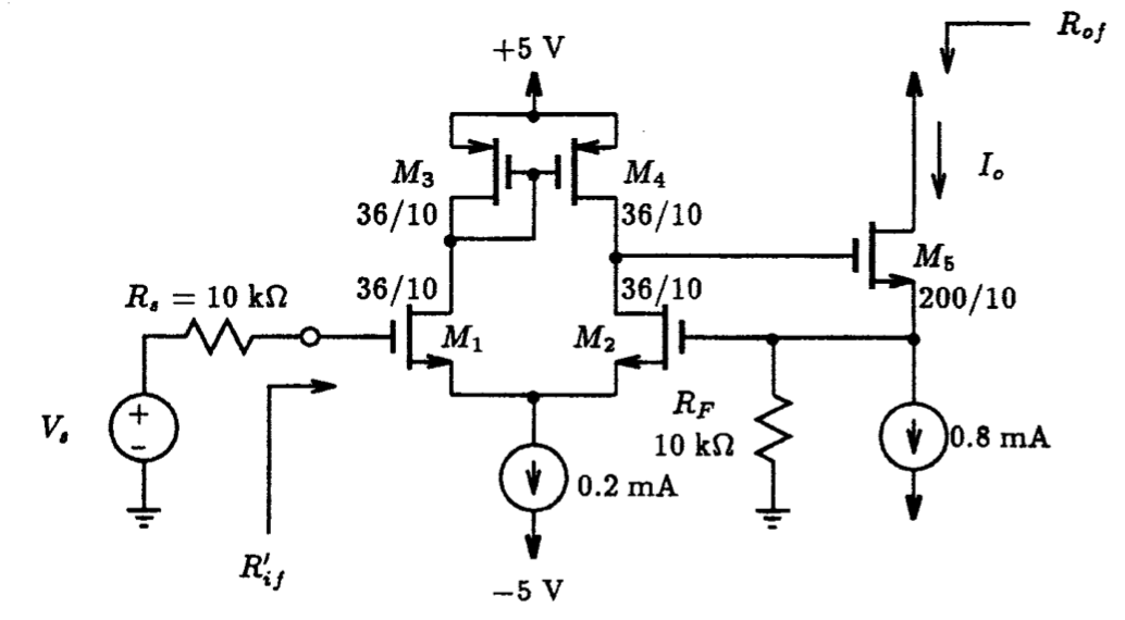
P8.7
8.7. Fig. P8.7 shows a circuit for a voltage-to-current converter employing series-series feedback via resistor Rf. The MOSFETs have the dimensions shown and mnCOX=20 mA/V2, |Vt|=1 V, and |VA|=100 V. Use feedback analysis, together with Spice, determine A, beta, Af=Io/Vs, Rif’ and Rof’. Compute the value of Io/Vs using Spice and compare this to Af.
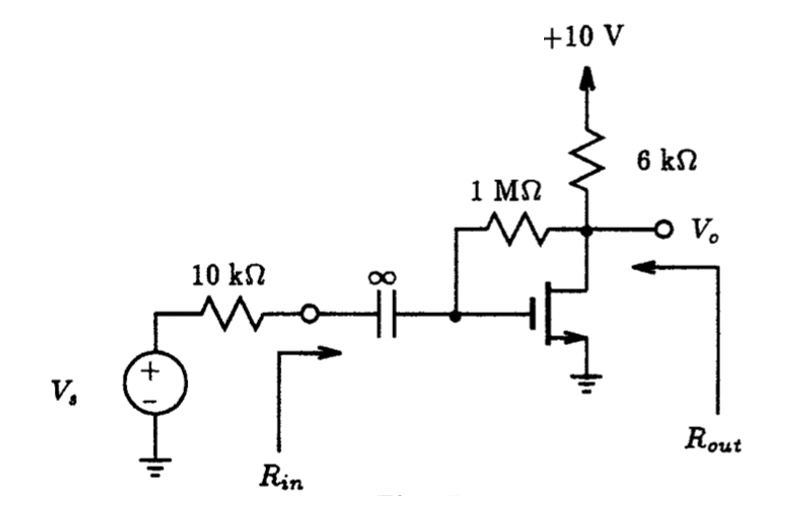
P8.8
8.8. For Vt=2 V and mnCOX=0.5 mA/V2, find the voltage gain Vo/Vs, the input resistance Rin, and the output resistance Rout of the circuit in Fig. P8.8 using feedback analysis in conjunction with Spice. Verify your results by direct analysis.


P8.9 P8.10
8.9. For the circuit of Fig. P8.9, use the feedback method, in conjunction with Spice, to find the voltage gain Vo/Vs, the input resistance Rif’, and the output resistance Rof’. The op-amp has open-loop gain m= 104 V/V, Rid=100 kOhm, Ricm=¥ and r0=1 kOhm.
8.10. Figure P8.10 shows how shunt-series feedback can be employed to design a current amplifier utilizing an op-amp. Using the feedback analysis method in conjunction with Spice, find the closed loop gain Io/Is, the input resistance (excluding Rs), and the output resistance (excluding RL) for the case: open-loop voltage gain of op-amp = 104 V/V, Rid=100 kOhm, op-amp output resistance = 1 kOhm, Rs=RL=10 kOhm, r=100 Ohm, and Rf=1 kOhm.
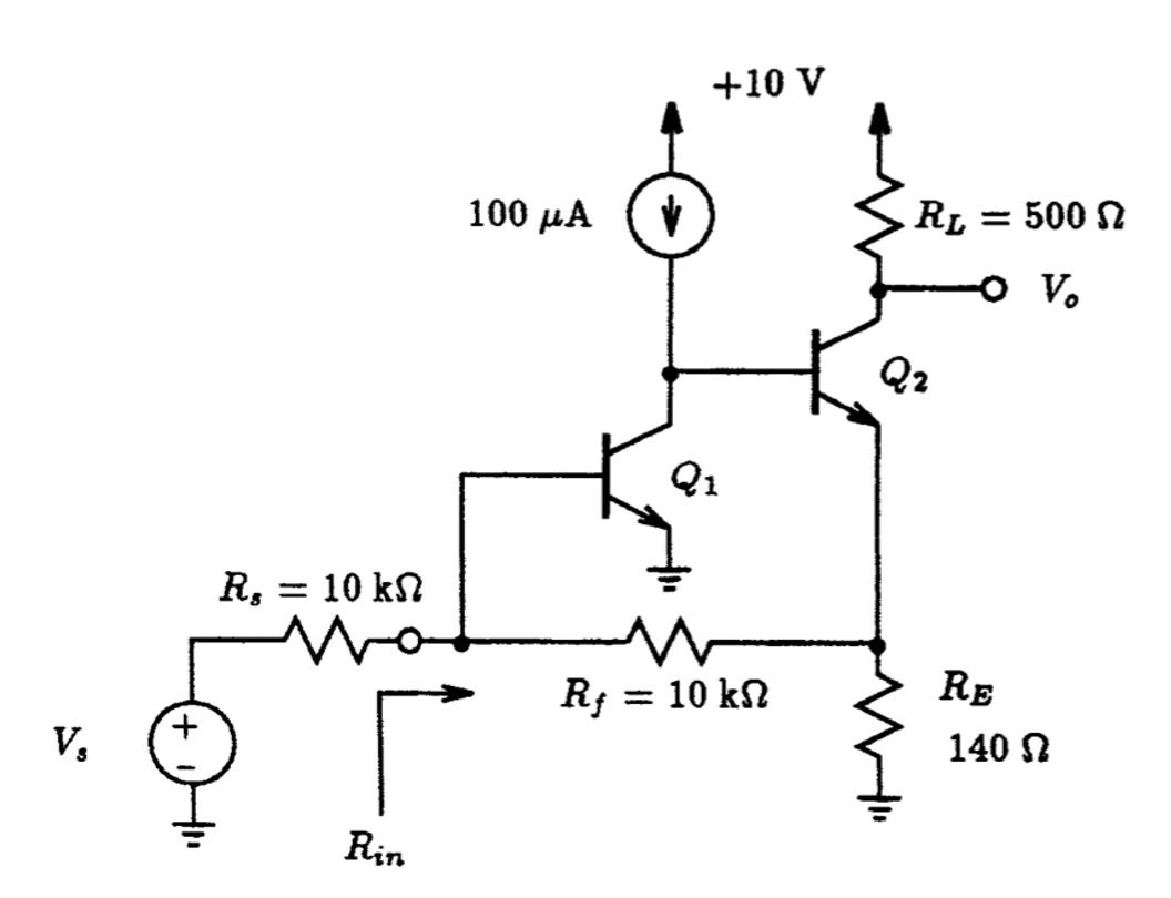
P8.11
8.11. For the amplifier circuit in Fig. P8.11, assuming that Vs has a zero-dc component find the dc voltages at all nodes and the dc emitter currents of Q1 and Q2. Let the beta=100. With the aid of Spice, use feedback analysis to find Vo/Vs and Rin.
8.12. Determine the loop gain of the amplifier in Fig. P8.2 by breaking the loop at the gate of M2, and finding the return voltage across the 100 kOhm resistor (while setting Vs to zero). The devices have |Vt|=1 V, mnCOX=1 mA/V2, and hfe=100. The Early voltage magnitude for all devices (including those that implement the current sources) is 100 V. Determine the output resistance Rof’.
8.13. Consider repeating Problem 8.12 above, but this time break the loop at the base of Q3 and terminate the loop by the resistance seen looking into the base of Q3. How does the loop gain compare to that found in Problem 8.12.
8.14. For the voltage amplifier seen in Fig. P8.3, determine the loop gain using the method of open- and short-circuit transfer functions.
8.15. Determine the loop gain of the amplifier circuit shown in Fig. P8.7 using: (a) the method of breaking the loop at the gate of M2 and terminating the loop with the proper impedance, and (b) the method of open- and short-circuit transfer functions. How do the results compare?
8.16. For the circuit in Fig. P8.11 calculate the loop gain and then find the input resistance Rin. Assume that the BJTs have hfe=100.

P8.17
8.17. A single-pole dc amplifier has an equivalent circuit representation shown in Fig. P8.17. If this amplifier is operated in a loop whose frequency-independent feedback factor is 0.1, with the aid of Spice, determine the low-frequency gain, the 3-dB frequency, and the unity-gain frequency of the closed-loop amplifier. Compare these results to those of the open-loop amplifier. By what factor does the single pole shift?
8.18. For the feedback amplifier described above in Problem 8.17, plot both the magnitude and phase of the loop gain. Is the amplifier stable? Confirm your conclusions by performing a transient analysis of the closed-loop amplifier subjected to a one-volt step input signal.

P8.19
8.19. An amplifier has a dc gain of 105 and poles at 105 Hz, 3.16 x 10⁵ Hz, and 106 Hz. An equivalent circuit representation of this amplifier is shown in Fig. P8.19. Using Spice, plot the magnitude and phase of the voltage gain of this amplifier, then answer the following questions. What is the value of beta, and the corresponding closed-loop gain, for which a phase margin of 45° is obtained?
8.20. Consider synthesizing an amplifier whose open-loop gain A(s) is given by

Plot its magnitude and phase response using PSpice. If this amplifier is to be used in a feedback configuration where the feedback factor beta is independent of frequency, find the frequency at which the phase shift is 180°, and find the critical value of beta at which oscillation will commence. Confirm your conclusion using a Spice transient analysis.

P8.21
8.21. A two-pole amplifier for which Ao=103 and having poles at 1 MHz and 10 MHz has a small-signal equivalent circuit model shown in Fig. P8.21. Assuming that this amplifier is to be connected as a differentiator, what is the smallest differentiator time-constant for which the operation is stable? Base your decision on the 6 dB/octave rate-of-closure rule. What are the corresponding gain and phase margins?
P8.22
8.22. The op-amp in the circuit of Fig. P8.22 has an open-loop gain of 105 and a single-pole rolloff with w3dB=10 rad/sec.
(a) Plot the Bode plot for the loop gain using Spice.
(b) Find the frequency at which |Abeta|=1 and find the corresponding phase margin.
8.23. An op-amp designed to have a low-frequency gain of 105 and a high-frequency response dominated by a single pole at 100 rad/sec, acquires, through a manufacturing error, a pair of additional poles at 10,000 rad/sec. Using Spice, plot the magnitude and phase response of the open-loop gain. At what frequency does the total phase shift reach 180°? At this frequency, for what value of beta, assumed to be frequency independent, does the loop gain reach a value of unity? What is the corresponding value of closed-loop gain at low frequencies?
8.24. For the situation described in Problem 8.23, with the aid of Spice, obtain Nyquist plots of the loop gain for beta=0.1 and 10-3 between the frequency range of 1 Hz to 100 MHz.